Loader
Rigid Circuits - Technosystem Sp. z o.o.
16070
page-template-default,page,page-id-16070,bridge-core-2.5.7,ajax_fade,page_not_loaded,,qode-theme-ver-24.2,qode-theme-bridge,qode_header_in_grid,wpb-js-composer js-comp-ver-7.2,vc_responsive
 

Rigid Circuits

Production documentation of printed circuits consists of:

  • Gerber files of the PCB project with drilling files,
  • laminate specification taking into account the stack-up,
  • information on additional requirements such as Tg (glass transition temperature), base material or impedance check.

While designing a stack-up of a multi-layer printed circuit, additional factors due to the technological limitations of the production process should be taken into account. One should also strive for the stack-up to be symmetrical, because it will avoid problems with uncontrolled bending of the laminate after the production or assembly process.


The final thickness of the laminate


– for 4-layer lamellas it is 0.4mm
– for a 6-layer laminate, it is 0.7mm
– for an 8-layer laminate, 0.9mm
– for a 10-layer laminate it is 1.2mmm
– for a 12-layer laminate, it is 1.5mm

In the case of lamellas with a HAL pad surface coating (HASL), the minimum PCB thickness cannot be less than 0.8 mm – due to the high temperature of the process, the risk of bending of the laminate increases.


Core and Prepreg dielectric layers


The suggested number of core layers (laminate core) in the multilayer circuit is calculated according to the formula L / 2 – 1, where L is the number of Cu layers. And so for a 4-layer stack-up laminate, one of the core layers (between layers L2 and L3) and 2 prepreg layers (between L1 and L2 and L3 and L4) is constructed. For 8-layer PCBs, 3 core layers are used, 12 layers of 5 core layers.

Typical stack-up designs for multilayer printed circuits::


Typical layered layers have limited application in the case of PCB production on special materials, such as ROGERS or ISOLA. The production specifications on such materials contain additional requirements, such as line impedance control and differential pairs. In such cases, the dielectric thicknesses are selected to meet the impedance requirements. We always confirm the final stack-up project with our clients.

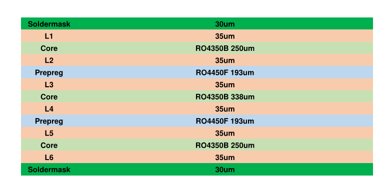
An example of the implementation of a printed circuit on ROGERS RO4350B material with impedance control of differential pairs on external layers.


Stack-up 6-layer PCB, ROGERS RO4350B

The final thickness of the laminate 1.5mm, thickness Cu 35um

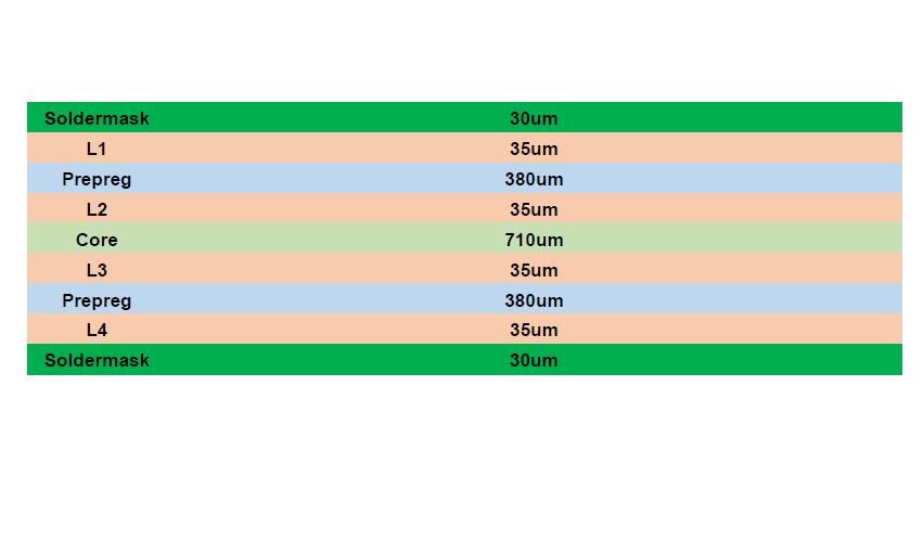
In the case of production of prototype 4-layer printed circuits with an express deadline, we use a stack-up based on NanYa NP140 material. The final thickness of the printed circuit at a Cu 35um thickness is 1.55mm.

Stack-up of a 4-layers PCB, final thickness of laminate 1.55mm, thickness of Cu 35um

– for express delivery

The distribution of Cu on the layers of printed circuits


In multilayer circuits, the copper in the layer should be evenly distributed. This will reduce the risk of laminate delamination after the production process or during component assembly. The distribution of copper on neighboring layers should also be balanced. The risk of delamination increases if, for example, the L1 layer is 80% thick and L2 is only 20%. Another factor to consider is the difference in Cu thickness between neighboring Co values in the PCB. This difference cannot be greater than 35um. Stack-up construction is not recommended, where for example the Cu thickness on the L3 layer is 35um and L4 105um.

Uneven distribution of Cu on the layer affects the process of galvanic thickening of copper on external layers (plating process). In the copper thickening process, the Cu ions will concentrate on the isolated pads, resulting in a higher Cu thickness than in places where the copper distribution is similar. For this reason, it is important to clearly and precisely define the requirements for the final copper thickness on the srface layers.

The basic base values for the Cu thickness of the materials we offer are 18um, 35um, 70um, 105um and 140um. On special request, we offer materials with thicker base copper. The thickness of copper obtained as a result of galvanic processes may oscillate between 18um and 35um. This means that for 18um base copper after the plating process, we get about 40um, and for the base 35um thickness – about 70um.

Minimum Cu thicknesses after galvanic processes on external layers according to IPC – 6012C standard “Qualification and Performance, Specification for Rigid, Printed Boards”.”.


Base thickness absolute minimum Cu after plating according to IPC after plating according to IPC Acceptable reduction

obwody_sztywne_1
obwody_sztywne_2
obwody_sztywne_3